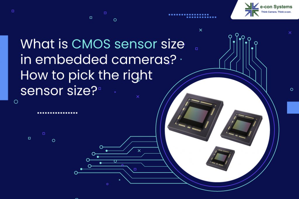
CMOS Image Sensors: The Technological Heartbeat of Modern Digital Photography and Visual Content Creation

In the dynamic world of digital imagery, from the breathtaking wallpapers that adorn our screens to the intricate stock photos fueling creative projects, the unsung hero at the core of nearly every capture device is the image sensor. Specifically, Complementary Metal-Oxide-Semiconductor (CMOS) image sensors have revolutionized how we perceive and interact with visual information, paving the way for the high-resolution, aesthetic, and emotionally resonant photography that defines Tophinhanhdep.com’s diverse collections.
Once considered a mere curiosity, CMOS technology has matured into the dominant force in digital imaging, outperforming traditional charge-coupled devices (CCDs) in versatility, power efficiency, and integration capabilities. This article delves into the intricate workings of CMOS image sensors, exploring their design, functionality, and the profound impact they have on the quality of images we capture, process, and share on platforms like Tophinhanhdep.com.
Unveiling the Core: Introduction to CMOS Image Sensors

The advent of solid-state imaging devices, primarily CCDs and CMOS image sensors, marked a pivotal moment, threatening to eclipse traditional recording technologies like film and video tubes. While both technologies emerged in the 1970s, CMOS sensors initially lagged in performance. However, by the early 1990s, significant advancements in CMOS design led to smaller pixel sizes, reduced noise, more capable image processing algorithms, and larger imaging arrays. Today, CMOS is ubiquitous, found in everything from microscopes to digital cameras, scanners, and even astronomical telescopes.
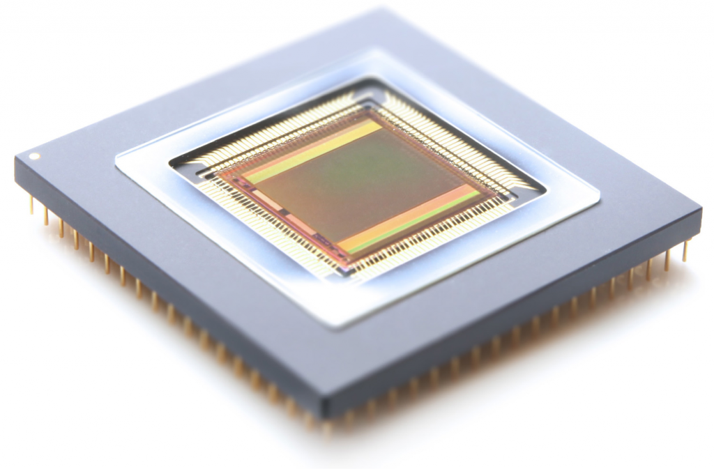
At its essence, a CMOS sensor is an electronic chip designed to convert photons (light particles) into electrons, which are then processed digitally. This conversion leverages the photoelectric effect: when photons interact with crystallized silicon, they promote electrons from the valence band into the conduction band. The term “CMOS” refers to the manufacturing process itself, rather than a specific imaging technology, highlighting its deep roots in semiconductor fabrication.
One of the major advantages of CMOS sensors over their CCD counterparts is their remarkably low power consumption and the ability to operate from a single-voltage power supply. CCDs, by contrast, often require multiple supply voltages and consume significantly more power. This efficiency makes CMOS sensors ideal for portable devices and embedded vision systems, enabling continuous operation crucial for capturing vast libraries of content for Tophinhanhdep.com’s themed collections, from nature’s subtle beauty to vibrant abstract art.
The fundamental building block of any digital image sensor is the photodiode, often referred to as a pixel. When visible light hits the specially doped silicon, a proportional number of electrons are released based on the light’s wavelength and intensity. These electrons are collected in a “potential well” during the integration (exposure) period. In CMOS sensors, this accumulated charge is converted into a voltage directly within the pixel. This voltage, or the equivalent charge in CCDs, then passes through an analog-to-digital converter (ADC), forming the digital electronic representation of the imaged scene. The efficiency of this conversion, known as sensitivity, is determined by the photodiode’s maximum charge capacity, its photon-to-electron conversion efficiency, and its ability to retain charge without leakage.
In optical microscopy, or any photographic setup, light gathered by a lens system is focused onto the sensor surface, which comprises a two-dimensional array of these photodiodes or pixels. The size of this array and the dimensions of individual pixels directly dictate the spatial resolution of the sensor. While inherently monochromatic, responding only to the total electron count, CMOS sensors achieve color imaging through ingenious methods. This is typically done by passing incident light through sequential red, green, and blue filters, or more commonly, by depositing miniature transparent polymeric thin-film filters in a mosaic pattern over the pixel array. This foundational capability allows Tophinhanhdep.com to offer images across the full spectrum of colors, supporting everything from vibrant backgrounds to subtly shaded aesthetic photography.
Anatomy of the CMOS Photodiode
A significant architectural advantage of CMOS image sensors is their capacity to integrate a multitude of processing and control functions directly onto the sensor integrated circuit itself. Beyond the primary task of photon collection, these integrated features include timing logic, exposure control, analog-to-digital conversion, shuttering, white balance, gain adjustment, and even initial image processing algorithms. This extensive on-chip integration makes a CMOS integrated circuit resemble a random-access memory cell more than a simple photodiode array.
The most prevalent CMOS designs employ Active Pixel Sensor (APS) technology, where each pixel incorporates both a photodiode and a readout amplifier. This enables the conversion of accumulated charge into an amplified voltage within the pixel, which is then transferred sequentially along rows and columns to the analog signal-processing section of the chip. Each pixel, therefore, contains a photodiode alongside a triad of transistors: one to convert accumulated electron charge to a measurable voltage, another to reset the photodiode (draining charge), and a third to transfer the voltage to a vertical column bus for readout. This design facilitates simple x,y addressing techniques for reading signals from individual pixels, a capability not inherent in older CCD technology.
A typical CMOS image sensor, for instance, might feature an active image area of 640x480 pixels, blanketed by an ordered layer of red, green, and blue-dyed polymeric filters, each precisely sized to fit over an individual photodiode. To further enhance photon collection, these filtered photodiodes often sit beneath a miniature positive meniscus lens array, known as a microlens array. These tiny lenses serve to focus incident light directly into the photosensitive area of the photodiode, increasing efficiency. On-chip analog signal processing circuitry collects and interprets these signals, sending them to adjacent analog-to-digital converters for transformation into digital data. The sensor also handles clock timing for the entire charge generation, voltage collection, transfer, and measurement cycle, along with preliminary image processing and output.
A closer inspection of the photodiode array often reveals a sequential mosaic pattern of red, green, and blue filters, famously known as the Bayer filter pattern. This pattern is designed to capture color information from broad-bandwidth illumination. It’s arranged in quartets, typically with an emphasis on green filters (two green for every one red and one blue), reflecting the human eye’s peak sensitivity in the 550-nanometer (green) region of the visible spectrum. This intelligent design ensures that Tophinhanhdep.com’s nature photography and aesthetic images render colors as vividly and accurately as the human eye perceives them.
However, a challenge arises from this pixel architecture: a significant portion of each pixel (often around 70%) is occupied by support transistors (amplifier, reset, row select), which are relatively opaque to visible light photons. This means only a small fraction (e.g., 30%) of the pixel area is actually photosensitive, leading to a reduced “fill factor.” This reduced fill factor can result in a loss of sensitivity and a lower signal-to-noise ratio, impacting dynamic range. Microlens arrays help mitigate this by focusing light onto the photosensitive regions, effectively doubling photodiode sensitivity in some cases, though they too can exhibit wavelength and angle selectivity.
Capturing Color and Reconstructing Images
The journey from light hitting a CMOS sensor to a fully rendered digital image involves complex processes, especially concerning color. Since CMOS sensors are inherently monochromatic, capturing color information requires specialized filtering and subsequent digital reconstruction. This is where the intricacies of image processing truly shine, transforming raw sensor data into the vibrant visuals seen on Tophinhanhdep.com.
Mosaic Filter Arrays and Image Reconstruction
As discussed, the most common method for color capture in CMOS sensors is through a mosaic filter array, predominantly the Bayer filter pattern. This pattern, with its unequal distribution of color filters (twice as many green as red or blue), might seem to pose a problem for accurate color reproduction at the individual pixel level. After all, a pixel with a green filter only “sees” green light directly. However, the human visual system plays a crucial role here: spatial resolution is primarily determined by the luminance (brightness) component of an image, not the chrominance (color). Our brains seamlessly integrate coarse color information with fine spatial detail.
Furthermore, Bayer filters have broad wavelength transmission bands with significant overlap. For example, yellow light (around 585 nm) can be transmitted by both red and green filters, and even partially by blue filters. This allows spatial information from various spectral regions to pass through, ensuring that each color retains a considerable degree of spatial detail. This subtle interplay between sensor design and human perception is key to capturing the high-resolution, detailed images demanded by Tophinhanhdep.com’s stock photo and digital art sections.
Once a raw image, consisting of a mosaic of red, green, and blue values from individual pixels, is acquired, it must be converted into a standard Red, Green, Blue (RGB) format. This crucial step, known as demosaicing or color interpolation, employs sophisticated algorithms (such as nearest neighbor, linear, cubic, or cubic spline techniques) to estimate the missing color values for each pixel. For instance, to determine the red and blue values for a green pixel, the algorithm averages the color values of its neighboring red and blue pixels, alongside their intensity. These algorithms, often executed directly on the integrated circuit post-capture, produce an image that accurately represents the original scene. While effective, they can sometimes introduce artifacts like aliasing at sharp edges or in areas of rapid color/intensity transitions.
To further enhance quantum efficiency and spectral response, some CMOS designers are exploring color filter arrays based on subtractive primaries (cyan, yellow, magenta – CMY) instead of additive primaries (RGB). CMY filters offer increased sensitivity and stronger signals due to reduced light absorption compared to RGB filters, and they are typically applied in a single, superior light-transmitting layer. The trade-off is a more complex color correction matrix required to convert CMY data into the RGB values needed for display or printing. While this conversion can introduce additional noise, the enhanced sensitivity often offsets these processing challenges, contributing to the rich, vibrant imagery featured in Tophinhanhdep.com’s aesthetic and inspirational collections.
Understanding Noise and Enhancing Image Quality
Despite their many advantages, CMOS image sensors have historically faced challenges with noise—unwanted variations in the electrical signal that can degrade image quality, leading to “grainy” or distorted visuals. Modern sensor technology has made immense strides in carefully integrating signal processing circuitry alongside the image array, significantly dampening many noise sources and dramatically improving CMOS performance. However, a comprehensive understanding of various noise types and their remedies is essential for achieving the pristine, high-resolution images expected from Tophinhanhdep.com’s photography.
Sources and Remedies of Noise
Several types of noise can plague CMOS image sensors:
- Fixed Pattern Noise (FPN): This artifact arises from manufacturing variations in amplifier transistor gain and offset across the array, producing a static, reproducible pattern in captured images. Modern CMOS designs largely mitigate FPN through design tuning of analog signal processing circuitry or by electronic subtraction of a dark image (flat-field correction). This ensures uniform backgrounds for wallpapers and stock photos on Tophinhanhdep.com.
- kTC (or Reset) Noise: Generated during the initialization or resetting of the photodiode, this noise is proportional to Boltzmann’s constant (k), operating temperature (T), and total capacitance (C) at the amplifier input. It can significantly limit the signal-to-noise ratio.
- Amplifier or 1/f Low-Frequency Noise: Also known as flicker noise, this is another common source of noise. Both reset and amplifier noise can be effectively controlled using correlated double sampling (CDS). This technique involves measuring the noise alone after reset, then measuring the signal plus noise after integration, and finally subtracting the first measurement from the second. This requires adding a “measuring” transistor to each pixel.
- Photon Shot Noise: This fundamental noise source is inherent in all image sensors (including CCDs) and manifests as a random pattern due to statistical fluctuations in the number of photons hitting each pixel and the temporal variation in the output signal. It’s the dominant noise for strong signals and appears as randomness, critical to manage for detailed digital photography and accurate visual design elements.
- Dark Current: This refers to signal charge (electrons) generated in the absence of any illumination. It’s highly temperature-sensitive and can vary significantly from pixel to pixel. Dark current can be reduced by cooling the sensor or by subtracting a stored dark frame from the captured image. Advanced fabrication techniques, such as pinned photodiode technology, also significantly reduce dark current. This involves applying a shallow P-type silicon layer to the N-well photosensitive region, confining electrons away from the surface. Pinned photodiodes also improve blue response by enhancing the capture of short-wavelength light.
- Thermal Noise: Induced by the transistors, capacitors, and bus lines within the pixel, thermal noise can be reduced by fine-tuning the imager bandwidth, increasing output current, or cooling the camera system. While expensive Peltier cooling is impractical for most consumer-grade CMOS sensors, limiting the bandwidth of each transistor amplifier through the readout sequence can help.
Effectively managing these noise sources is paramount for producing the high-quality, clean images vital for Tophinhanhdep.com’s offerings, particularly for high-resolution photography and visual design where clarity is paramount. The continuous advancements in noise reduction are key to enabling the rich dynamic range and crisp details seen in modern digital art and stock photos.
CMOS Pixel Architecture and Operational Sequence
The internal architecture of a CMOS pixel and the sequence of its operation are central to understanding its performance characteristics, including sensitivity, speed, and overall image quality. These architectural choices dictate how photons are converted into digital data, influencing everything from dynamic range to frame rate.
CMOS Pixel Architecture
Modern CMOS image sensors primarily utilize two basic photosensitive pixel element architectures: photodiodes and photogates.
- Photodiode Designs: Generally more sensitive to visible light, particularly in the short-wavelength (blue) region of the spectrum. They excel at directly converting light into charge within the photodiode itself.
- Photogate Devices: These often have larger pixel areas but a lower fill factor and poorer blue light response compared to photodiodes. However, photogates can achieve higher charge-to-voltage conversion gains and are easily adapted for correlated double sampling (CDS) for superior noise reduction, especially at low light levels. They often incorporate aspects of CCD technology for noise reduction, localizing charge accumulated under the photogate and performing a two-stage transfer to the output bus. This dual-sampling opportunity significantly improves noise performance.
While photogate designs offer reduced noise in low-light conditions, photodiode-based CMOS sensors are prevalent in mid-level consumer applications that prioritize cost-effectiveness and good performance without necessarily requiring extremely low noise or superior dynamic range. Both architectures benefit from the economical power requirements of CMOS technology, making them suitable for battery-powered devices or those powered by low-voltage computer interfaces, perfectly aligning with the accessibility needs for generating diverse content for Tophinhanhdep.com.
CMOS Image Sensor Operational Sequence
The process of image capture in a CMOS sensor follows a precise sequence:
- Reset: The process begins by initializing a reset transistor in each pixel. This drains any residual charge from the photosensitive region and reverse biases the photodiode, preparing it for a new exposure.
- Integration (Exposure) Period: Light interacts with the photodiode, producing electrons that are stored in a silicon potential well beneath the surface. This period determines the exposure time.
- Readout: Once integration is complete, a row-select transistor switches on, connecting the amplifier transistor in the selected pixel to its load. The electron charge in the photodiode is converted into a voltage by the source follower amplifier. This voltage appears on the column bus and is detected by a sense amplifier. This cycle repeats, reading out every row in the sensor to produce an image.
In most designs, the active pixel array is surrounded by optically shielded “black” pixels. These are crucial for black level compensation, where their average signal level is subtracted from the digital video output to account for temperature and time-dependent dark noise. This ensures accurate dark tones in Tophinhanhdep.com’s abstract photography and sad/emotional imagery.
CMOS sensors can employ different readout modes. Progressive scan reads every pixel consecutively, starting from the top-left to the bottom-right. Interlaced scan reads pixels in two alternating fields (odd rows, then even rows).
Electronic shuttering is another critical function. While adding transistors to each pixel for a true global shutter can impact the fill factor, many modern CMOS sensors achieve global shutter functionality, exposing the entire array simultaneously. This is essential for capturing fast-moving objects without distortion or “jello effect,” a common artifact of rolling shutters (where rows are exposed sequentially). For Tophinhanhdep.com’s high-speed photography or capturing dynamic nature scenes, global shutter CMOS sensors are indispensable.
Dynamic range, a key performance metric, is determined by the maximum number of signal electrons a photodiode can accumulate (charge capacity) divided by the total sensor read noise (noise floor). A higher dynamic range allows the sensor to simultaneously capture both the dimmest and brightest intensities within a single image, critical for photography with challenging lighting conditions. This directly impacts the richness and detail of Tophinhanhdep.com’s beautiful photography.
One of the most powerful capabilities of CMOS image sensors is their ability to achieve very high frame rates. This allows for the recording of time-lapse sequences and real-time video, often exceeding 1000 frames per second in specialized imagers. Furthermore, windowing (or window-of-interest readout) enables selective reading and processing of only a chosen portion of the pixel array. This dramatically expands image processing possibilities, allowing for electronic pan, zoom, accelerated readout, and tilt operations directly on the chip. These features offer immense flexibility for digital photography, video creation, and specialized visual design applications on Tophinhanhdep.com.
The Future of CMOS in Digital Imaging
The rapid evolution of CMOS image sensor technology is deeply intertwined with advancements in semiconductor manufacturing. Fabricated on well-established standard silicon processes in high-volume wafer plants, CMOS sensors benefit from the ability to integrate digital logic circuits, clock drivers, counters, and analog-to-digital converters onto the same silicon foundation as the photodiode array. This allows CMOS sensors to participate in “process shrinks,” moving to smaller linewidths with minimal redesign, similar to other integrated circuits. However, achieving low-noise, high-performance imaging often requires specific modifications to the standard CMOS fabrication process, as techniques optimal for logic chips might lead to high dark currents or poor blue response in image sensors.
Pixel sizes have continuously shrunk over the years, moving from 10-20 micron pixels in the mid-1990s to 6-8 micron, and now down to 3-4 micron for multi-megapixel chips. This miniaturization, driven by the demand for compact electronic imaging devices like smartphone cameras and surveillance systems, requires production on increasingly narrow fabrication lines (e.g., 0.25-micron or narrower). Smaller linewidths enable more transistors to be packed into each pixel while maintaining acceptable fill factors, paving the way for advanced on-chip features such as in-pixel analog-to-digital converters, full-color processing, and interface logic that enhance flexibility and dynamic range.
While some CMOS fabrication plants may lack the specialized steps for adding color filters and microlens arrays, these capabilities are becoming increasingly common as market demands for high-quality imaging grow. Optical packaging techniques, crucial for imaging devices, also necessitate clean room environments and specialized equipment not typically found in standard logic chip manufacturing, which can add to initial production costs.
The application landscape for CMOS image sensors has expanded exponentially. From their growing presence in fax machines, scanners, security cameras, and low-end consumer cameras in the late 1990s, CMOS sensors are now integral to cell phones, barcode readers, optical mice, automotive systems, industrial inspection, fluid dynamics, and medical diagnostics. Their ability to capture high-frame-rate sequential images makes them invaluable for real-time analysis and recording. Although CCDs still hold niches in some extremely high-end scientific applications, CMOS image sensors are continually finding new homes and advancing the frontier of visual capture.
For Tophinhanhdep.com, the continuous evolution of CMOS technology means an ever-improving supply of high-resolution, low-noise, and dynamically rich imagery. These sensors are the unseen force enabling stunning wallpapers, detailed stock photos, vibrant digital art, and the raw material for creative photo manipulation. As CMOS technology progresses, it promises even more sophisticated tools for visual design, enhanced capabilities for AI upscalers to process and refine images, and endless inspiration for thematic collections and trending styles, cementing its role as the indispensable foundation of our digital visual world.